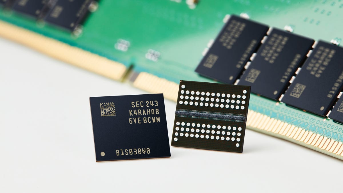
Samsung stated on Thursday that it has begun mass manufacturing of its double knowledge fee 5 (DDR5) DRAM made with a 12-nanometer (nm) class course of node. The tech big introduced the event of the 16Gb DDR5 DRAM in December final yr.
The beginning of the mass manufacturing of the 12nm DRAM, which makes it essentially the most superior amongst DRAMs out there, at a time when the reminiscence chip trade goes by a downturn, exhibits that Samsung, the world’s largest reminiscence chipmaker, intends to take care of its management within the sector and extra.
In line with Samsung, the brand new chip, in comparison with the prior era, has energy consumption diminished by 23% whereas its wafer productiveness was up by 20%, that means 20% extra chips could be produced out of a single wafer because the chip is smaller than the prior era.
The tech big stated the diminished energy consumption from the 16Gb DDR5 DRAM will permit server and knowledge heart operators to scale back their power consumption and carbon footprint.
The chip additionally has a most velocity of seven.2Gbps, which implies it could actually course of 60GB in round a second, and is geared toward knowledge facilities, AI and new computing functions.
The 12nm node was achieved due to Samsung’s use of a brand new high-k materials that permits the chip to precisely distinguish variations in knowledge indicators.
The DRAM has been verified for compatibility with AMD in December already and Samsung stated it was collaborating with extra international IT firms on the present time.